cover
coverY
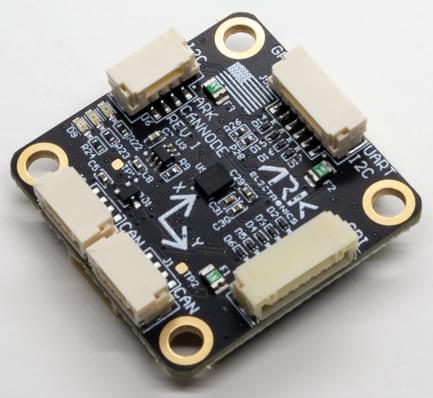
../../.gitbook/assets/ark_can_3.jpg
0
ARK CANnode is an open source generic DroneCAN node that includes a 6 degree of freedom IMU. Its main purpose is to enable the use of non-CAN sensors (I2C, SPI, UART) on the CAN bus. It also has PWM outputs to expand a vehicle's control outputs in quantity and physical distance.
Find 3D models and case files at https://github.com/ARK-Electronics/ARK_CANNODE
Open Source Schematic and BOM Sensors
Bosch BMI088 6-Axis IMU or Invensense ICM-42688-P 6-Axis IMU
STM32F412CGU6 MCU
Two Pixhawk Standard CAN Connectors
Pixhawk Standard I2C Connector
Pixhawk Standard UART/I2C Connector (Basic GPS Port)
Pixhawk Standard SPI Connector
PWM Connector
10 Pin JST GH
8 PWM Outputs
Matches Pixhawk 4 PWM Connector Pinout
Pixhawk Standard Debug Connector
Small Form Factor
LED Indicators
USA Built
Power Requirements
5V
Current dependent on connected peripherals
The ARK CANnode is connected to the CAN bus using a Pixhawk standard 4 pin JST GH cable. For more information, refer to the CAN Wiring instructions.
You will see both red and blue LEDs on the ARK CANnode when it is being flashed, and a solid blue LED if it is running properly.
If you see a solid red LED there is an error and you should check the following:
Make sure the flight controller has an SD card installed.
Make sure the ARK CANnode has ark_cannode_canbootloader installed prior to flashing ark_cannode_default.
Remove binaries from the root and ufw directories of the SD card and try to build and flash again.
Ark CANNode Configuration On the ARK CANnode, you may need to configure the following parameters:
Parameter
Description
CANNODE_TERM CAN built-in bus termination.
Pin Number Signal Name Voltage 1 5V 5.0V 2 CAN_P 5.0V 3 CAN_N 5.0V 4 GND GND
Pin Number Signal Name Voltage 1 5V 5.0V 2 CAN_P 5.0V 3 CAN_N 5.0V 4 GND GND
UART1/I2C1 - 6 Pin JST-GH Pin Number Signal Name Voltage 1 5.0V Out (500mA) 5.0V 2 USART1_TX 3.3V 3 USART1_RX 3.3V 4 I2C1_SCL 3.3V 5 I2C1_SDA 3.3V 6 GND GND
Pin Number Signal Name Voltage 1 5.0V Out (500mA) 5.0V 2 I2C1_SCL 3.3V 3 I2C1_SDA 3.3V 4 GND GND
Pin Number Signal Name Voltage 1 5.0V 5.0V 2 SPI2_SCK 3.3V 3 SPI2_MISO 3.3V 4 SPI2_MOSI 3.3V 5 SPI2_CS_1 3.3V 6 SPI2_CS_2 3.3V 7 GND GND
Pin Number Signal Name Voltage 1 Pulled up to 3.3V through a 1.5kΩ resistor 3.3V 2 TIM2_CH1_PWM1 3.3V 3 TIM2_CH2_PWM2 3.3V 4 TIM2_CH3_PWM3 3.3V 5 TIM3_CH1_PWM4 3.3V 6 TIM3_CH2_PWM5 3.3V 7 TIM3_CH3_PWM6 3.3V 8 TIM3_CH4_PWM7 3.3V 9 TIM4_CH2_PWM8 3.3V 10 GND GND
Pin Number Signal Name Voltage 1 3.3V 3.3V 2 USART2_TX 3.3V 3 USART2_RX 3.3V 4 FMU_SWDIO 3.3V 5 FMU_SWCLK 3.3V 6 GND GND