connections are not being followed through bus definitions across views #3678
Description
Current Behaviour
The setup:
The (custom) arduino_uno_for_shields part has multiple bus definitions. Among them are entries to connect the digital IO pins D11, D12, D13 to the ICSP1 header pins for MOSI, MISO, and SCK. The part contains connector definitions for all of those pins, but the ICSP pins deliberately do not include schematicView entries. Since they are bused together, and schematic view is a logical view, any connection (on any view) to D11, D12, D13 should also be a connection to the matching ICSP1 header pins. More on should in a moment.
The dragino_lora_shield part also includes multiple bus definitions. Here, the ICSP pins are NOT linked with the digital IO pins. However, both the ICSP header and associated digital IO pins ARE bused to pins on a configuration header.
Another bus definition in the uno part, is for the 5 ground pins. 4 of those pins exist on the shield (there is no ICSP2 header here), but they are left as individual pins, not grouped together by a bus definition.
Holding mouse down on the bused pins of the individual parts in breadboard view shows the pin, and each of the bused pins, as yellow. In the current implementation, the pcb view for the uno is blank, but the shield exists, and the bused pins light up with mouse down on one of them. The schematic view has definitions for both parts, but currently none of the bused pins have more than a single representation, so individual part buses are not readily visible here.
When the shield board is dragged over the uno part in breadboard view, the matching pins turn blue, showing a valid connection. When (aligned correctly and) released, those shield pins turn green, plus the extra header pins that are (both) bused within the shield part and are (now) connected to one of the uno pins. That is the configuration header pins that are bused to the digital IO or ICSP(1) header pins. In addition, the Arduino digital IO side of the enable jumper headers light up. The shield side of those jumpers stay red, but mouse down on them turns the bused shield digital IO pins yellow.
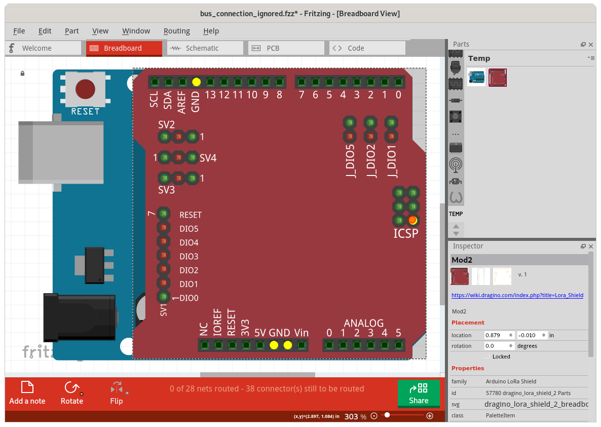
With the shield mounted on the uno, mouse down on any of the bused connections turns the whole group yellow. Of note here are the ICSP(1), configuration header, and Arduino digital IO pins. Mouse down on (for example) D13 turns D13, ICSP1 SCK, SV2 pin 1, and SV2 pin 3 yellow. The uno part has D13 bused to ICSP1 SCK, the shield part has D13 bused to SV2 pin 3, and ICSP SCK bused to SV2 pin 1. With the shield part aligned/connected with the uno part, the 2 D13 pins are connected, and the 2 ICSP SCK pins are connected. So all 6 of the pins are connected. In breadboard view, they actually show as connected using mouse down on one of them.
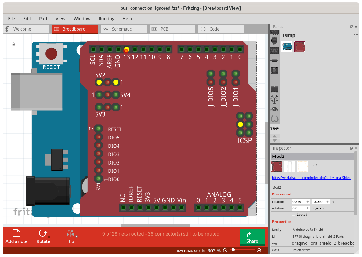
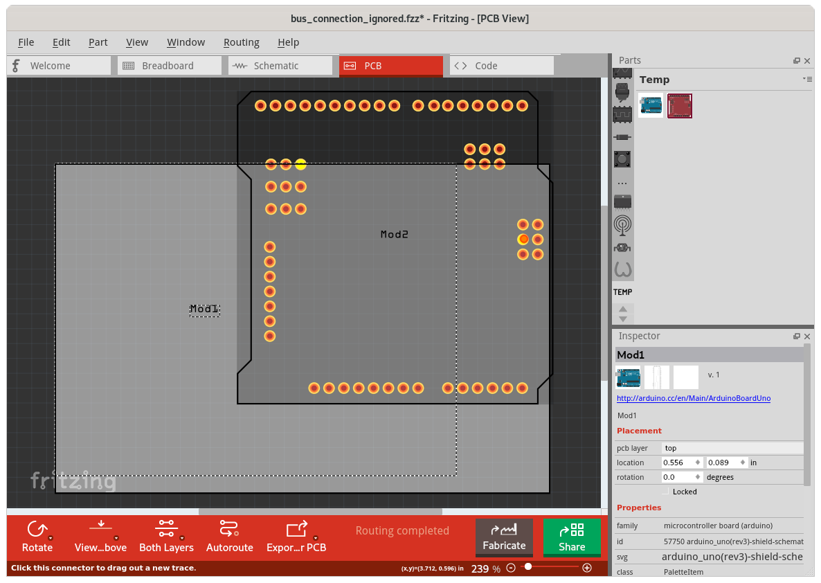
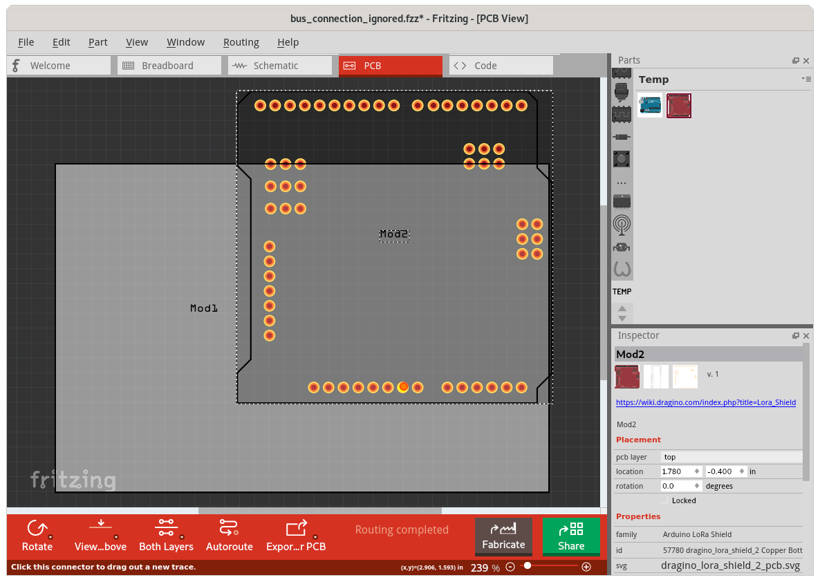
All of that looks correct, but PCB view does not show quite the same information. There are no uno connection pins to click on, but the pins for the shield are available. Mouse down on D13 here turns only it and SV2 pin 3 yellow. The connection to ICSP SCK, via the shield to uno D13 connection, uno bus from D13 to ICSP1 SCK, uno ICSP1 SCK to shield ICSP SCK is not seen, nor the extension of that to SV2 pin 1 through the bus on the shield. A simpler failure is the ground connections. Each of the 4 GND pins on the shield is connected to the matching GND pin on the uno, and all of the uno GND pins are grouped in a single bus. However, mouse down on the pcb view shield GND pins does not show any of the others as connected.

The schematic view has issues as well. The GND pins of the uno and shield are not shown as connected. The 3V3 and 5V pins are connected, as shown by the ratsnest lines. The 3V3 is easy. There is only a single 3V3 pin on each of the uno and shield parts, and they are connected by the placement of the shield part on the uno in the breadboard view. The 5V is a bit more complex. There are 3 5V pins on the uno part grouped into a bus. Each of the 2 5V pins on the shield is connected to a matching 5V pin on the uno by the shield placement in breadboard view, plus the single schematic view 5V pin for each part is matched to the main 5V pin. The 2 5V schematic pins are hooked to connections that are directly connected in breadboard view. Like the 3V3 connection, no bus needs to be referenced to show the linkage.
As described above, the 5 uno part GND pins are grouped into a bus, but the 4 shield part GND pins are left separate. For the schematic view shield part, the single GND pin is associated with the GND pin that is beside (in breadboard view) VIN. The single uno part schematic view GND pin is associated with the second power header gnd pin, which is beside (in breadboard view) 5V. In schematic view they are not connected. No ratsnest line, and nothing else turns yellow with mouse down on the pins.
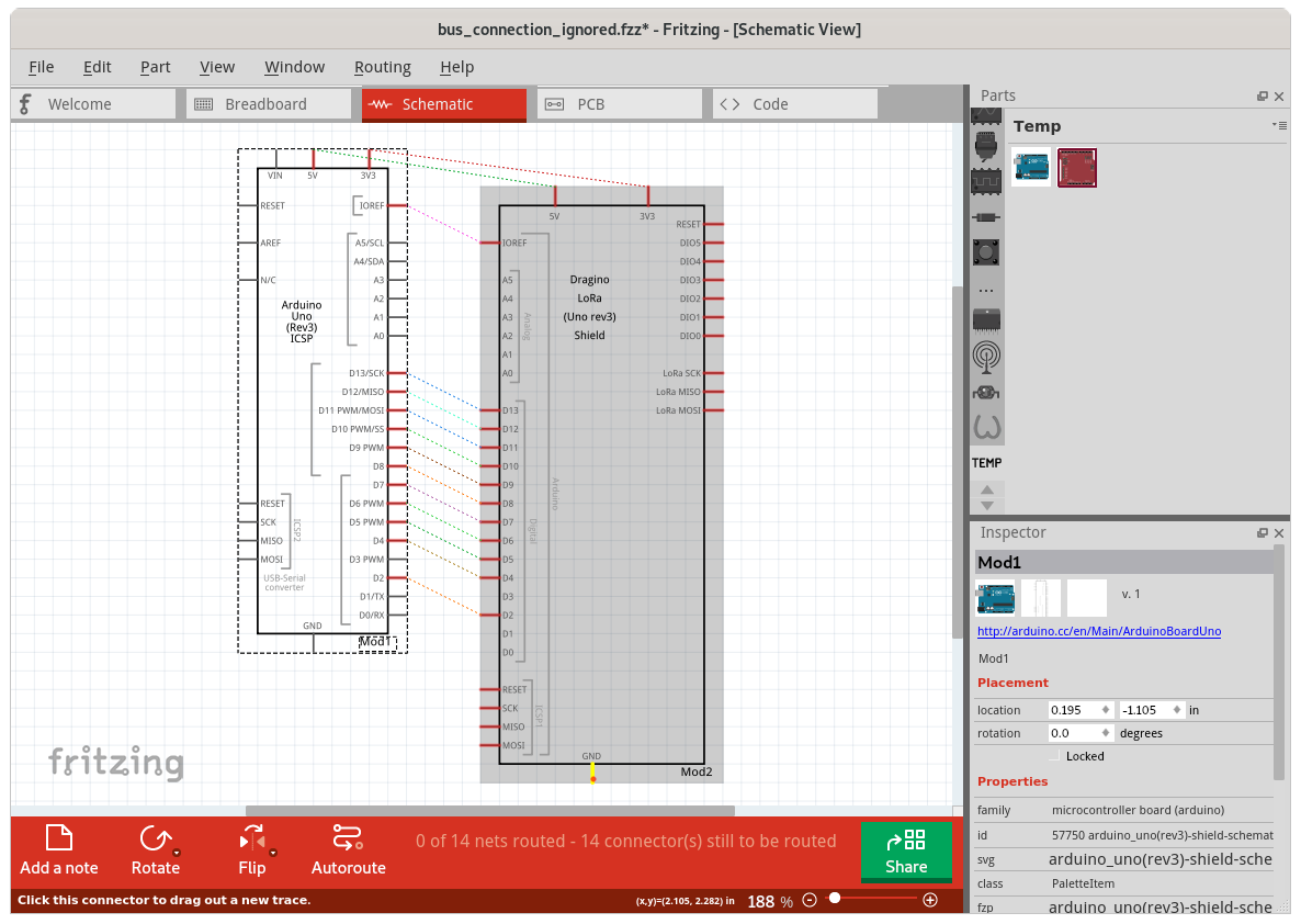
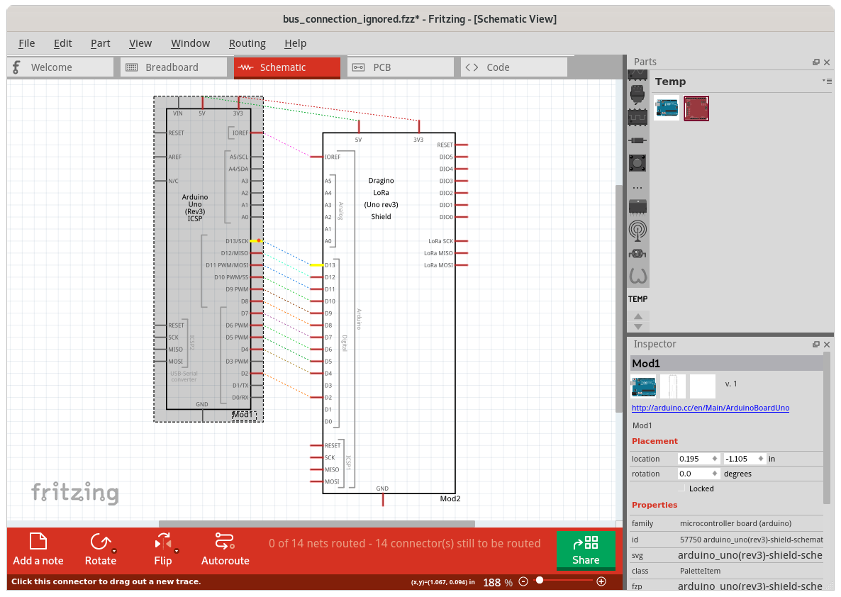
As shown on breadboard view, the 4 ICSP SCK pins are connected and grouped together. On schematic view, that is not visible. Mouse down on one of the D13 pins only turns it and the other D13 pin yellow. Mouse down on the shield ICSP SCK pin only turns it yellow.

The fact that the 2 physical pins are tied together, as defined by the bus definition, is not being seen as creating a connection between the GND pins in schematic view. Same for PCB view. The connections are not being followed from PCB view pin, to connected part pin, through connected part bus, back to another pin on PCB view. The schematic view case is simpler, since there is at least a GND pin from the bused group in the view, even it is not the one that is directly connected in the breadboard view. The pcb view does not have a GND (or any) pin for the uno. But in both cases, the internal connectivity information should be providing a path through the physically connected pins, and the bused pins that are grouped with them.
Here is the sketch with custom parts that were used to generate the screenshot images. Remove the trailing .zip to open it.
bus_connection_ignored.fzz.zip
Build:
Version 0.9.5 (dCD-548-17-g694c4a08 2020-04-27) 64 [Qt 5.12.7]
Same symptoms with Fritzing 0.9.4.2019-12-01.CD-498
Operating System:
Fedora 31 Workstation
5.6.11-200.fc31.x86_64
Steps to reproduce:
- Open the example fzz sketch
- Mouse down on various pins in each view to see what is connected, and examine the ratsnest lines (only) in schematic view
Expected Behaviour
Every view should use the part bus definition information, and connections to the associated pins (in any view) when checking what should be connected by ratsnest or shown as connected on mouse down.
The schematic should show a ratsnets wire between the part GND pins
Mouse down on either GND in schematic view show show the other GND as connected
Mouse down on Either D13 or SCK in schematic view should show all 3 pins as connected
Mouse down on any of the shield GND pins in PCB view should show all 4 as connected
Mouse down on any of D13, SV2.1, SV2.3, ICSP SCK of shield part in PCB view should show all of them as connected
The GND pins in schematic