Minimal inkjet printhead driver IC exploration using the
GF180MCU open PDK, with a focus on:
- ⚡ high-voltage device layout
- 🧩 mixed-signal integration
| Language | GitHub Pages 🌐 | GitHub 💻 |
|---|---|---|
| 🇺🇸 English |
The core technical documentation for this project lives under the docs/ directory and is published via GitHub Pages.
-
🌐 GitHub Pages (rendered docs)
👉 Design Documentation (GitHub Pages) -
📂 docs/ (design rationale, architecture, HV layout notes)
👉 GitHub Repository – docs/
All layout- and GDS-oriented discussions are intentionally centralized there.
This repository explores a minimal inkjet printhead driver IC architecture implemented on the GF180MCU open PDK.
Primary goals:
- ⚡ Understanding high-voltage device usage in GF180
- 📐 Investigating layout strategies for HV + logic coexistence
- 🔀 Studying mixed-signal partitioning for inkjet drivers
- 🧱 Building a reusable architectural reference
This is not a production-ready design,
but a technical exploration and educational reference.
- Process: GF180MCU (Open PDK)
- Voltage Domains:
- Low-voltage logic (core / IO)
- High-voltage devices for inkjet actuation
- Design Style:
- Mixed-signal
- Layout-driven learning
- Minimal functional blocks
- High-voltage MOS device selection and constraints
- Level-shift and isolation concepts
- Simple driver stage topologies
- Layout considerations:
- Spacing rules
- Guard rings
- Substrate noise awareness
- Mixed-signal floorplanning concepts
Inkjet printhead drivers sit at the intersection of:
- ⚡ High-voltage analog devices
- 🧠 Digital control logic
- 📐 Tight layout and reliability constraints
GF180MCU provides a rare opportunity to study this
using a fully open PDK.
This repository serves as a sandbox for that purpose.
- ✅ Flow feasibility evaluation completed
- 📐 Manual layout exploration phase (HV-focused)
- 🧩 GDS targets identified (device- and structure-level)
This project has completed evaluation of automated digital flows
and has transitioned to layout-centric exploration.
No attempt is made to converge toward a production-ready IC.
The outcome is the identification of feasible and infeasible
design regions at the GDS level.
This project did not fail.
It successfully identified the practical design boundary between:
- automated digital P&R flows, and
- manual mixed-signal / high-voltage IC design
using the GF180MCU open PDK.
- ❌ GF180MCU Open PDK is not compatible with OpenLane’s OpenPDK flow
- Fully automated synthesis → P&R → GDS
is not a viable approach for this process
Inkjet printhead drivers inherently require:
- High-voltage device utilization
- Mixed-signal integration (logic + HV analog)
- Layout-driven decision making
These characteristics place such designs outside the effective scope of fully automated digital flows.
- Manual / semi-manual layout exploration
- High-voltage device and isolation studies
- Mixed-signal floorplanning
- Educational and architectural research
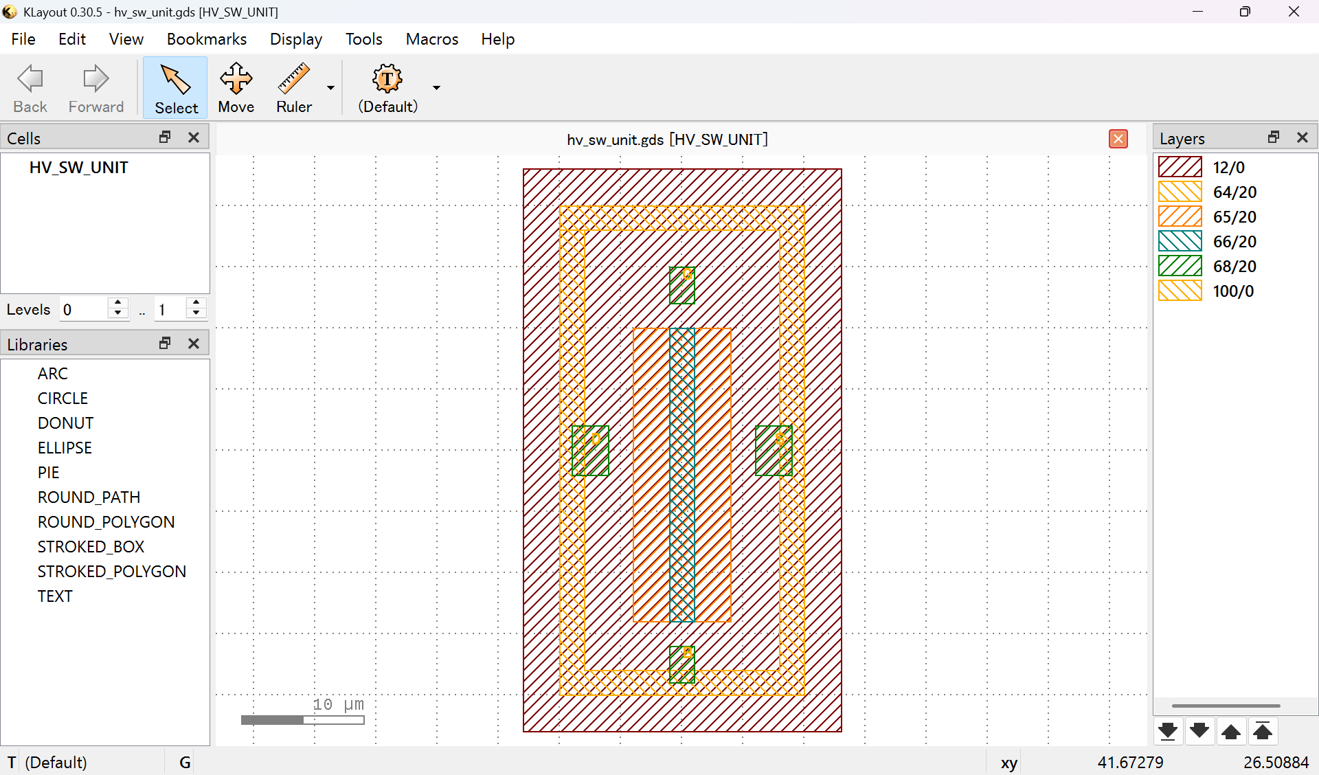
The following image shows a representative high-voltage switch unit GDS generated during this exploration.
It demonstrates:
- DNWELL isolation
- Continuous P+ guard ring
- Central HV device structure
- Explicit D / G / S / B pin exposure
| 📌 Item | Details |
|---|---|
| Name | Shinichi Samizo |
| Expertise | Semiconductor devices (logic, memory, high-voltage mixed-signal) Thin-film piezo actuators for inkjet systems Printhead productization, BOM management, ISO training |
| GitHub |
| 📌 Item | License | Description |
|---|---|---|
| Source Code | MIT License | Free to use, modify, and redistribute |
| Text Materials | CC BY 4.0 or CC BY-SA 4.0 | Attribution required; share-alike applies for BY-SA |
| Figures & Diagrams | CC BY-NC 4.0 | Non-commercial use only |
| External References | Follow the original license | Cite the original source properly |
Suggestions, improvements, and discussions are welcome via GitHub Discussions.