Extended Memory (Flash cartridge)
On the GameTank, addresses at 0x8000 and above will access hardware in the cartridge slot. For simple EEPROM cartridges up to 32KB the address will be directly mapped to the address in the EEPROM chip. However to access the data in a 2MB cartridge we need to manage additional address bits.
The 2MB cartridge has a shift register that can set these higher address bits, and we talk to this shift register through four GPIO pins on the cartridge slot. These pins are mapped to Output Register A on the 6522 VIA, accessed at 0x2801. In this document I'll go over the structure and reasoning of the 2MB flash cartridge and then what code is needed to interface with it.
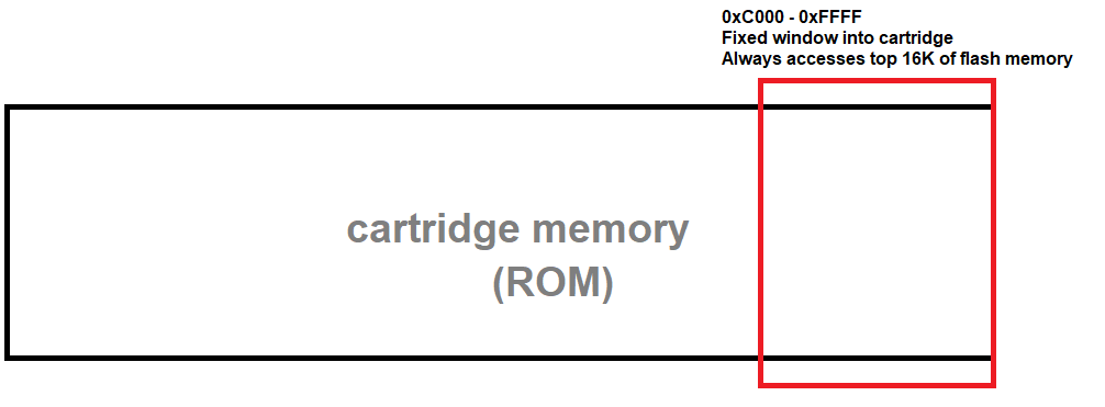
When the GameTank boots, it needs guaranteed access to the location of the RESET vector or else it won't start the software reliably. So the memory space of the cartridge is separated into two sections that provide a window into the data on the flash chip. The section containing the RESET and interrupt vectors is fixed in place. So the address range from 0xC000 - 0xFFFF will always ALWAYS access the last 16 kilobytes of the flash chip.
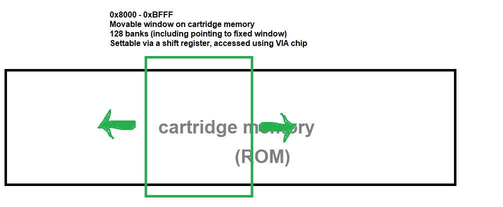
For additional code and data, we look at 0x8000 - 0xBFFF which maps a sliding window into the flash memory. The aforementioned shift register is used to select which of the 128 16k-sized chunks of flash memory that this range will look at.
In the GameTank there are 16 GPIO pins controlled by the VIA chip. Twelve of these are exposed on a port on the back of the console, and four of them are in the cartridge port. For the purposes of the 2MB Flash Cartridge three of these are used as a one-way serial port.
Here are some definitions I use at the top of an assembly file to help with this:
VIA = $2800
ORB = 0
ORA = 1
DDRB = 2
DDRA = 3
T1C = 5
ACR = $B
PCR = $C
IFR = $D
IER = $E
First we make sure the correct VIA pins are in output mode:
	LDA #%00000111
	STA VIA+DDRA
Then this subroutine will take the value in the Accumulator and feed it to the shift register:
ShiftHighBits:
	STA temp
	LDA #$FF
	STA VIA+ORA

        LDA temp
        ROR
	ROR
	ROR
	ROR
	ROR
	ROR
	AND #2
	ORA #%00000100
	STA VIA+ORA
	ORA #1
	STA VIA+ORA

	LDA temp
	ROR
	ROR
	ROR
	ROR
	ROR
	AND #2
	ORA #%00000100
	STA VIA+ORA
	ORA #1
	STA VIA+ORA

	LDA temp
	ROR
	ROR
	ROR
	ROR
	AND #2
	ORA #%00000100
	STA VIA+ORA
	ORA #1
	STA VIA+ORA

	LDA temp
	ROR
	ROR
	ROR
	AND #2
	ORA #%00000100
	STA VIA+ORA
	ORA #1
	STA VIA+ORA

	LDA temp
	ROR
	ROR
	AND #2
	ORA #%00000100
	STA VIA+ORA
	ORA #1
	STA VIA+ORA

	LDA temp
	ROR
	AND #2
	ORA #%00000100
	STA VIA+ORA
	ORA #1
	STA VIA+ORA

	LDA temp
	AND #2
	ORA #%00000100
	STA VIA+ORA
	ORA #1
	STA VIA+ORA

	LDA temp
	ROL
	AND #2
	STA VIA+ORA
	ORA #1
	STA VIA+ORA

	ORA #4
	STA VIA+ORA

	RTS
With this subroutine defined we can shift to any sector of Flash ROM by setting the accumulator and jumping to the routine:
	LDA #5
	JSR ShiftHighBits
On the regular 2MB flash cartridge, the highest bit of this register is unused. However a recently developed Flash+SRAM cartridge uses this bit to determine whether to access battery-backed RAM used for savegames and other user data.
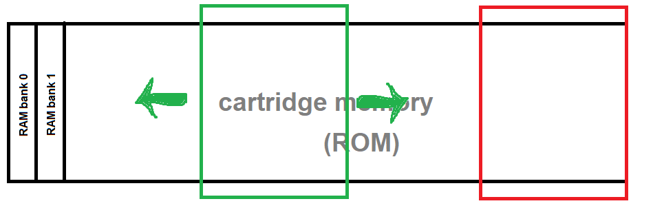
The fixed memory range 0xC000 - 0xFFFF behaves the same as before, but the movable window will now access RAM if the eighth bit is zero. The seventh bit determines which of the two RAM halves to access, since the SRAM is only 32 kilobytes.
To summarize the mapping of the shift register values:
- 0x00 - 0x3F = All map to the same 16k bottom half of the cartridge RAM
- 0x40 - 0x7F = All map to the same 16k upper half of the cartridge RAM
- 0x80 - 0xFF = Each maps to their own section of flash memory
For a 2MB cartridge without flash, the ranges 0x00 - 0x7F will map to the same bank plus 0x80. So 0x00 == 0x80, 0x11 == 0x91, etc.
The emulator and the flashing tool will treat a ROM file as containing all the banks lined up end-to-end, in order. When building ROMs for the 2MB cartridge I typically build separate 16K bank files and then concatenate them together, and generate a filler file for the unused banks. Writing programs that have code spanning multiple banks is a little more complicated, though setting up a build config for cc65 can simplify things a lot.
For VASM I'd just write the program in 16K and manually pick addresses to use for data in other banks. Here's an example from the makefile for the Bad Apple demo
	vasm6502_oldstyle -dotdir -wdc02 -Fbin badapple.asm -o badapple.gtbs
	truncate -s 928235 tmp.padding
	cat bad_apple_frames.dat tmp.padding badapple.gtbs > badapple.gtr
	rm tmp.padding
In this example truncate is used to genarate padding for 56 unused flash banks and 10,731 bytes unused in one of the banks.