This repository is for my digital storage oscilloscope project.
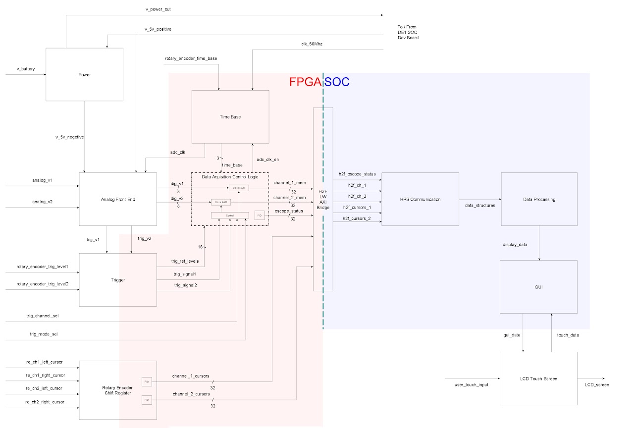
This project is a year long project with two other students to build a two channel digital storage oscilloscope using the Cyclone V FPGA SOC. The FPGA half of the chip is used to aquire data, and the Soc(called the HPS in documentation) half of the chip is used to display that dat onto a GUI. The two halfs of the chip communicate over a pair of axi bridges. These bridges let the FPGA access HPS memory, and give the Soc access to registers on the FPGA. This is a yearlong project and is ongoing. The project will be complete during spring term 2020.
ghrd_top.sv is the top level module for the logic on the FPGA.
soc_system.qsys is the qsys system for this project.
soc_system.v is the top level module for the qsys system.
Code for each module is split into folders.
There is also a folder with a schematic and PCB gerbers I designed for this project.
Bellow is a more in depth overview of the project and what I did for it.
I am responsible for three blocks within the system. The analog front end block, the trigger block, and the data aquesition controll logic block.
The analog front end block is repsonsible for filtering the two analog voltages that we are measuring with the scope, and for sending those voltages into adc's to be sampled. This block is completely on the PCB.
The trigger block is used to generate a trigger signal, that is used by the data acquisition control logic block to trigger the signals we are measuring. This block is partially on the PCB and partially on the FPGA. On the PCB there is a DAC and comparator. The DAC is used to generate a trigger voltage that is sent to a comparator. The DAC is controlled over SPI by the FPGA. The comparator compares the trigger voltage and the analog voltage of the wave we are measuring, and outputs a signal that is sent to the data aq contnrol logic block. There is also a pair of rotary encoders that are used to change the trigger level. On the FPGA there is logic which decodes the Rotary encoders, and that interfaces with the DAC over SPI.
The data acquesition block is responsible for storing data into memory that can be accesed by the Soc and displayed on a GUI. Inside this block there is a state machine that controlles the triggering process. This state machine looks at the trigger signal and uses it to determine how data is stored in memory. The memory used to store data is in the form of on chip dual port block ram within the FPGA. One port of the RAM is used by the FPGA to wirte samples into memory. This port is connected to a memory controller, which is controlled by the trigger state machine. The other port of the RAM is connected to the HPS through one of the HPS FPGA interfaces, and is used to let the soc read sample data out of memory to be displayed on the GUI. A description of the FPGA Soc interface is given bellow.
The HPS and FPGA interface through three axi bridges. An FPGA-to-HPS bridge, a heavywieght HPS-to-FPGA bridge and a lightweight HPS-to-FPGA bridge. The on chip RAM is connected to the HPS through the lightweight H2F bridge. This bridge is made up of slaves on the FPGA which are mastered by the HPS through the AXI bridge. This bridge lets the HPS read from and write to registers on the FPGA. In our design one port of the on chip RAM is connected to the h2f slaves on the FPGA, and can be read through the h2f lightweight axi bridge by the HPS. The adress space of the on chip RAM is mapped to a virtual address space, that can be pointed to by code on the HPS.